In another article, we have discussed the Bipolar Junction Transistor and the differences between NPN and PNP transistors. Transistor characteristic curve is a very useful thing to understand the basic principle and operation of a Transistor. In this article, we’re going to discuss the input and output characteristics of a Transistor. The main discussion is on the transistor characteristic curves of a BJT. There are three possible configurations of a transistor – common emitter (CE), common base (CB) and common collector (CC). In this article, we have used the CE configuration of the transistor.
Contents in this article:
- Characteristics Curves
- Circuit diagram to draw Input and output characteristics of Transistor
- Input Characteristics of Transistor
- Output Characteristics of Transistor
- Active Region
- Saturation Region
- Cut off region
- Inverted Region
Characteristics Curves
Characteristics curves are graphical plots indicating the variation of current with applied voltage. This is true for any electric and electronic circuit. Using these characteristics curves one can determine the operation of that circuit. In this article, we are going to discuss the input and output characteristics curves of a Bipolar Junction Transistor.
Circuit diagram to draw input and output characteristics curve of a BJT
One can draw the characteristics curves of a Transistor by using the following Transistor Amplifier circuit. Here, an NPN transistor is used in common emitter (CE) mode.
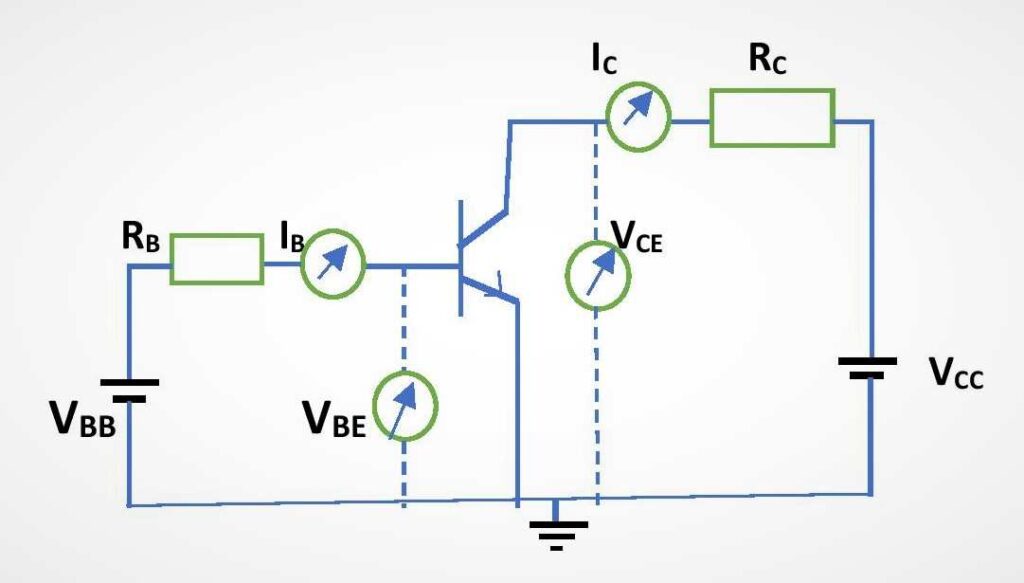
VBE is the input voltage, VCE is the output voltage, IB is the input current and IC is the output current. To measure input and output voltages and currents, two voltmeters and two ammeters are used in this circuit. One can use this circuit for practical purposes too. This circuit is also used for the transistor characteristics experiment. The experimental data is used to draw the transistor curves.
Input Characteristics of Transistor
The input characteristics curve is the graph that indicates the variation of input current with the input voltage. That means one needs to analyze the variation of base current (IB) with the base-to-emitter voltage (VBE). To draw IB vs VBE curve, the output terminal should be grounded. That means the collector terminal should be connected to the emitter terminal as the emitter is already grounded in CE mode. At this condition, the transistor behaves like a p-n junction diode. Therefore the IB vs VBE curve will be similar to the diode characteristics curve. Figure-1 gives the Input characteristics curve of a Transistor in CE mode.
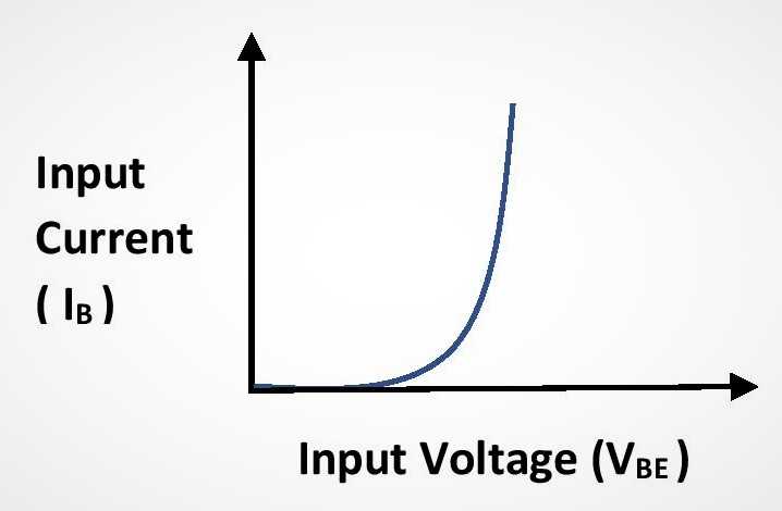
To draw IB vs VBE curve we need to collect the data for IB and VBE through the corresponding ammeter and voltmeter. Then we have to plot the curve with the help of these data. There is an exponential growth of base current with an increase in VBE.
Output Characteristics of Transistor
The output characteristics curve of a Transistor gives the variation of output current with the change in output voltage. In a common emitter transistor, the collector current is the output current and the collector-to-emitter voltage is the output voltage. Fig.2 shows the output characteristics curve of a Transistor.
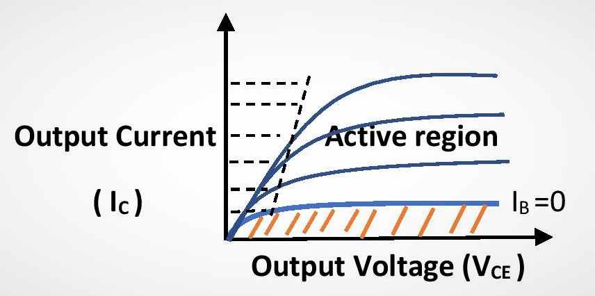
After collecting the data for IC and VCE through the corresponding ammeter and voltmeter one can easily plot the IC vs VCE curve. The graph shows a rapid increase in collector current at the beginning and then the collector current becomes almost constant. If VCE is increased further, the breakdown occurs and then the transistor may be damaged. One can divide the output curve into four regions –
- Active Region (the region in which output current becomes almost constant)
- Saturation Region (horizontal dotted lines (—-) in output curve indicates transistor saturation region)
- Cut-off region ( //// lines on the output curve indicate the cut-off region)
- Inverted region (appears after the breakdown which is not shown in the output curve)
Active Region of a Transistor
The region on the output curve of a transistor where the output current is almost constant and independent of the output voltage is the Active region of the Transistor. If the base resistance is greater than the maximum allowed value then the transistor operates in Active region. One can use Transistor as an Amplifier only if it operates in active region. To operate a transistor in active region, the emitter junction should be in forward bias and the collector junction should be in reverse bias.
Saturation region of Transistor
The saturation region is the region on the output curve of a transistor where the collector current increases rapidly with a slight increase in output voltage. To operate the transistor in the saturation region, the base resistance should be smaller than the maximum allowed value and both of emitter junction and collector junction should be in forward bias. In saturation region, a transistor acts like the ON stage of a switch.
Cut-off region of a Transistor
In the Cut-off region, the base current is almost zero. Therefore, the collector current also becomes zero even at a higher output voltage. To operate a transistor in the cut-off region, both of emitter junction and collector junction should be in the reverse bias condition. A Transistor acts like the OFF stage of a switch in the cut-off region.
Inverted region of a Transistor
This is the inverse of active region. A transistor will operate in inverted region if its emitter junction is in reverse bias and the collector junction is in forward bias. In this region, breakdown occurs and collector current increases rapidly. There is no major practical use of transistors in inverted region. Therefore, transistor operation in this region is rarely used. This region is not shown in the output diagram.
| Region of Operation | Emitter Junction biasing | Collector Junction biasing | Use of the transistor in this region |
| Active region | Forward Bias | Reverse Bias | As an Amplifier |
| Saturation region | Forward Bias | Forward Bias | As a Switch (ON stage) |
| Cut Off region | Reverse Bias | Reverse Bias | As a Switch (OFF stage) |
| Inverted region | Reverse Bias | Forward Bias | (Rarely used) |
This is all from this article on the Input and Output Characteristics curve of a Transistor. Here we learned how to draw input and output characteristics curves for a CE mode BJT transistor. Then we became to know the four regions in the transistor output curve and their uses. If you have any doubts or queries on this topic you can ask me in the comment section.
Thank you!
Related Posts:
- Bipolar Junction Transistor
- Transistor as a Switch
- Difference between NPN and PNP Transistor
- p-n junction diode
- Use of Zener diode as a voltage regulator
5 thoughts on “Input and output characteristics of a Transistor”
Comments are closed.