In the first two articles, we learned the basic things about semiconductor materials. Now, we have entered into the applications of Semiconductors. Semiconductor materials are used to develop many electronic devices. A p-n junction diode is one of those. In this article, I’m going to discuss the formation, characteristics curves, depletion layer, potential barrier, bias circuit diagram, working principle and uses of a p-n junction diode.
Contents of this article:
- P-n junction diode
- p-n junction diode formation
- Potential Barrier of p-n junction
- Depletion layer of p-n junction
- Bias circuit of p-n junction diode
- Expression for diode current
- I-V curve of p-n junction diode
- Ideality factor (η) of diode
- Peak Inverse voltage (PIV) of diode
- Uses of p-n junction diode
A p-n junction diode is a semiconductor substrate with p-type and n-type doping at its two sides. Obviously, at the p-side doping impurities are the Trivalent atoms and at the n-side, the doping impurities are the pentavalent atoms.
There are four basic techniques for manufacturing a p-n junction diode—
- Grown Junction technique
- Alloy Junction technique
- Epitaxial technique
- Diffusion technique
Formation of p-n junction diode:
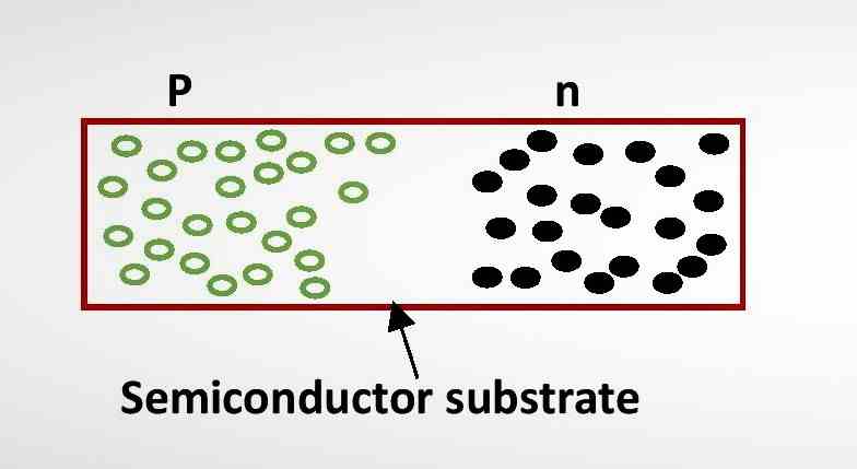
When two sides of a semiconductor substrate are doped with n-type and p-type respectively, the electrons from the n-side start to flow toward the p-side and the holes from the p-side start to flow toward the n-side, due to concentration gradients. This is called the diffusion of charge carriers. At a region, n-type and p-type become in contact and produce a junction. This junction of p-type and n-type semiconductors is called a p-n junction. It has two electrodes – positive (p-side) and negative (n-side) and hence it is also called a diode.
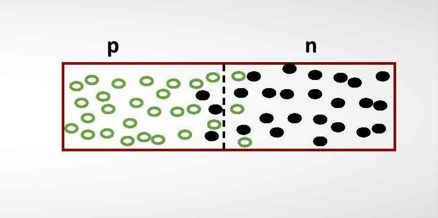
Potential Barrier in p-n junction:
When p-type and n-type atoms meet at the junction, recombination between some of the electrons of the n-side and holes of the p-side takes place. As both n-type and p-type atoms are neutral, then n-type atoms and p-type atoms that have contributed to recombination will lose electrons and holes respectively.
So, n-type donor atoms will become positively charged ions and p-type acceptor atoms will become negatively charged ions after the recombination. This recombination takes place at a small width at either side of the junction and only the atoms nearer to the junction contribute to recombination. Now, the n-side near the junction gets positive potential and the p-side near the junction gets negative potential. This potential difference across the junction opposes electrons and holes to move further across the junction. Because electrons cannot move from higher potential to lower potential and holes cannot move from lower potential to higher potential. Therefore, this potential difference across the p-n junction is called the Potential Barrier.
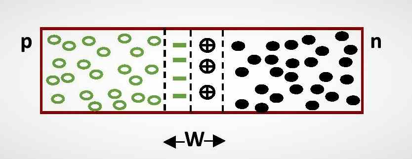
Depletion layer of p-n junction:
The depletion layer is the small region consisting of only minority ions extended at either side of the junction. There are no majority carriers inside the depletion region. In the above diagram, W is the width of the depletion layer of the p-n junction.
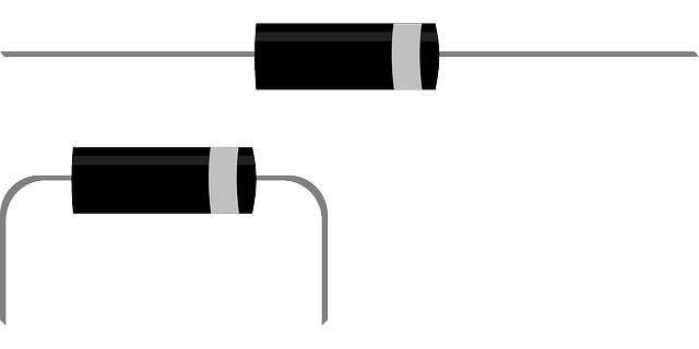
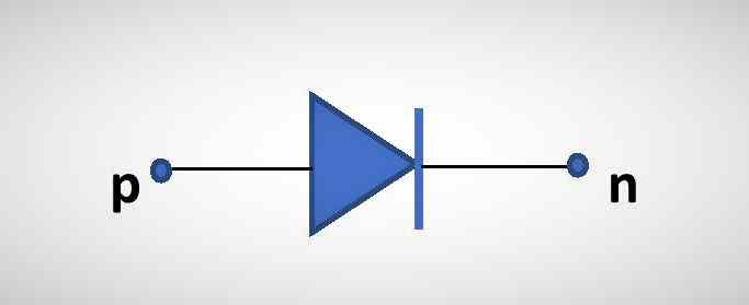
Symbol of p-n junction diode:
Biasing of p-n junction diode:
After the formation of the p-n junction, a potential barrier arises across the junction which opposes further charge flow through the junction. At equilibrium, there will be no current crossing the junction. Now, to get current through the junction carriers need sufficient energy to overcome the potential barrier at the junction and this energy can be supplied by applying an external voltage across the p-n junction. The process of applying the external voltage across the p-n junction is known as bias. A p-n junction can have two types of biasing – Forward bias and Reverse bias.
Forward Bias of p-n junction diode with circuit diagram:
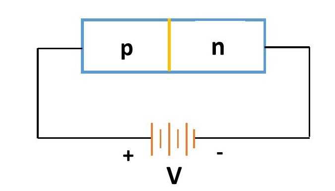
If we connect the positive terminal of a battery with the p-side of the diode and the negative terminal of the battery with the n-side of the diode, then the biasing is called Forward bias. Forward Bias (FB) allows the majority carriers to go forward i.e., when the diode is in forward bias, electrons will move from n-side to p-side and holes will move from the p-side to the n-side across the junction. In Forward Bias,
- Huge current flows across the junction
- The width of the depletion layer becomes smaller.
Reverse Bias of p-n junction diode with circuit diagram:
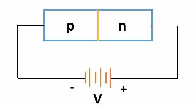
If we connect the positive terminal of a battery with the n-side of the diode and the negative terminal of the battery with the p-side of the diode then the biasing will be called the Reverse Bias (RB). In Reverse bias, the potential barrier increases, and majority carriers will experience more opposition to flow across the junction. However, the minority carriers will get the required energies to cross the junction as the reverse bias of p-n junction acts like the forward bias of minority carriers. Thus, in Reverse Bias,
- A very small current flows through the junction due to minority carriers.
- Width of the depletion layer increases.
Expression for diode current:
If V is the voltage across a p-n junction diode, then the expression for the current through the junction of the diode is, I = I0 [exp(eV/ηKT) – 1 ].
Here, T is the temperature and η is the ideality factor of the diode.
Diode Current in forward bias, I = I0 exp(eV/ηKT)
The Diode current in reverse bias is I = – I0 which is very small.
Working principle of p-n junction diode:
In the forward bias condition, a high current flows across the p-n junction diode and in the reverse bias condition a negligible current flows through the p-n junction. So, a p-n junction diode is active in forward bias condition and it is inactive or OFF in the reverse bias condition. That means a p-n junction diode transfers current or any signal from input to its output only in forward bias condition. This is the main working theory of the p-n junction diode. This principle can be verified by the characteristics curves of a p-n junction diode which are in the following sections.
p-n junction diode characteristics curve:
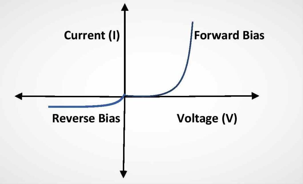
p-n junction diode has non-linear current-Voltage characteristics. It does not obey Ohm’s law and Kirchhoff’s law of current electricity. There are I-V curves of p-n junction diode below for both forward bias and reverse bias conditions. These are the characteristics of the PN junction diode or the characteristic curve of pn junction diode.
Forward bias characteristics of p-n junction diode:
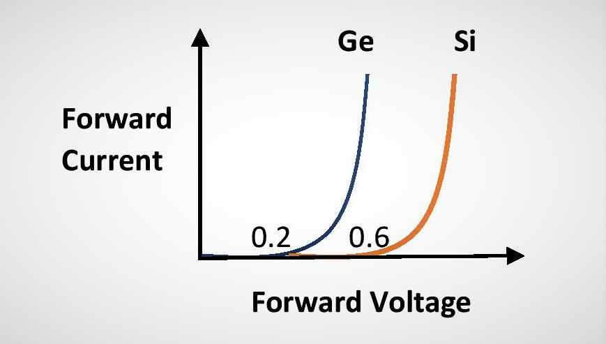
In the Forward bias, if the applied voltage exceeds the cut-in voltage (0.2 volts for Ge and 0.6 volts for Si) then current flows through the junction. The diode current increases exponentially to a very high value due to a further increment of forward bias voltage. The above diagram shows the i-v curve of p-n junction diode in forward bias.
Reverse bias characteristics of p-n junction diode:
In the reverse bias condition, very small diode current flows due to minority carriers only and this amount of current is almost independent of the reverse bias voltage.
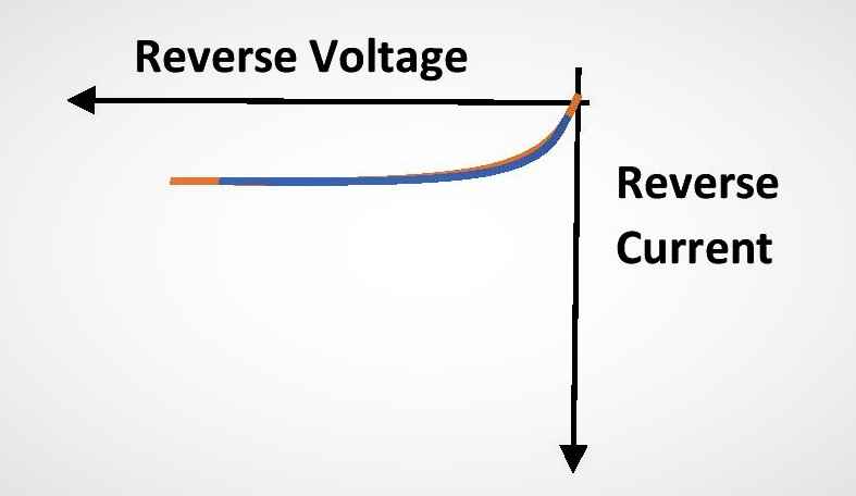
If we increase the reverse bias voltage further, the breakdown of the diode occurs at which the reverse bias current becomes very high. Unfortunately, diodes cannot withstand the breakdown region unless it is specially designed. Zener diode has a special design and some specifications such that it does not burn out even in the breakdown region.
Suggested Article: Zener diode and its use as a Voltage regulator.
I-V characteristics of Ideal Diode:
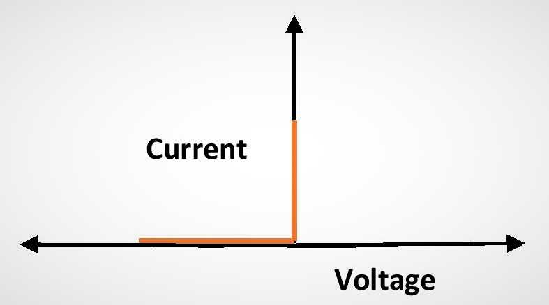
This is the I-V characteristic curve of the ideal diode. Ideally, a p-n junction diode should have zero cut-in voltage. Also, it should have zero internal resistance in Forward bias and infinite internal resistance in Reverse bias. So, the Diode current will be infinite even at zero forward bias voltage and there will be no diode current even in infinite reverse bias voltage.
Ideality Factor (η) of p-n junction diode:
The ideality factor (η) is a dimensionless parameter of a diode that determines the departure or deviation of diode characteristics from the ideal diode characteristics.
The ideality factor depends on the material, temperature and physical construction of the diode. For Ge, η=1 and for Si, η=2.
Peak Inverse Voltage (PIV) of diode:
Peak inverse voltage is the maximum reverse bias voltage that can be applied across the diode before entering in the breakdown region. So, after PIV, the diode enters in breakdown region and it can burn out at a high temperature that arises due to the sudden rise of the reverse bias current.
Uses of p-n junction diode:
A p-n junction diode has two major uses,
- As a switch
- As a rectifier to convert alternating current (AC) into direct current (DC).
Also, a p-n junction diode can be used as a circuit component in various electronic circuits.
In this article, we learned about the p-n junction diode, its circuit diagram, formation, characteristics curves and uses. This is all from this article. If you have any doubts on this topic you can ask me in the comment section.
Thank you!
Related posts:
- Use of Zener diode as voltage regulator
- Intrinsic and Extrinsic type of Semiconductor Material
- Bipolar Junction Transistor (BJT)
12 thoughts on “p-n junction diode – formation, biasing circuit & curve”
Comments are closed.