Bipolar Junction Transistor (BJT) is one of the very important electronic circuit components in the world of electronics. Scientist William Shockley discovered the first Transistor in 1948. Modern technology is very much progressive and many varieties of transistors have been discovered. These transistors are widely used in analog and digital electronics. In short, semiconductor diodes and transistors are the basic components of electronic devices. In this article, we’re going to discuss Bipolar Junction Transistors or BJTs, their properties, types and uses.
Contents of this Article:
- What is Bipolar Junction Transistor (BJT)?
- Types of BJT
- Construction of BJT
- Uses of BJT transistor
What is a Bipolar Junction Transistor (BJT)?
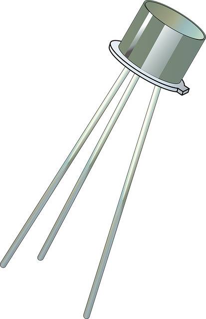
Bipolar Junction Transistor is a three-terminal electronic circuit component or device used to amplify the input signal at the output of an electronic circuit. It is made of semiconductor materials. One can fabricate a BJT by doping a semiconductor substrate with n-type and p-type materials alternatively into three parts. These three parts are the Emitter, Base and Collector regions of the transistor.
Types of Bipolar Junction Transistors
There are two types of BJT on the basis of doping in three regions-
- NPN Transistor
- PNP Transistor
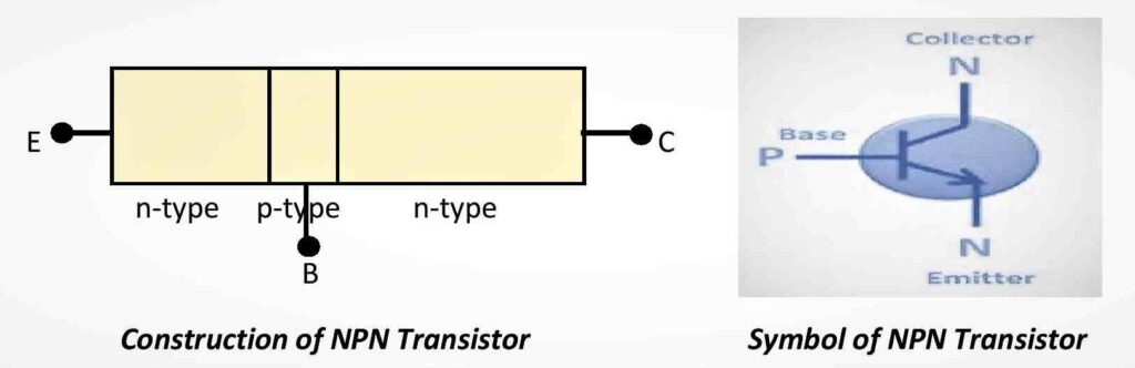
NPN Bipolar junction Transistor
When a p-type region is sandwiched between two n-type regions in a semiconductor substrate, an NPN transistor forms. The full form of NPN Transistor is Negative Positive and Negative Transistor. The negative and positive terms refer to the doping type of the three regions of the Transistor. The doping type of the Emitter and Collector are n-type and the doping type of the Base region is p-type. Thus, free electrons are the majority carriers in NPN Transistors.
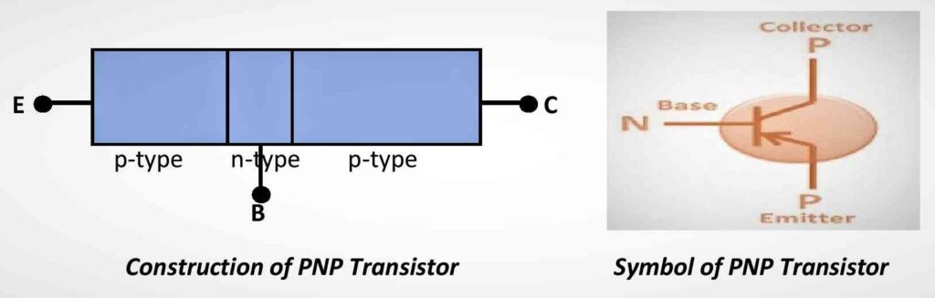
PNP Bipolar junction Transistor:
PNP Transistors can be constructed by inserting an n-type region between two p-type regions in a semiconductor substrate. The full name of PNP transistor is Positive Negative and Positive Transistor. In this type of BJT, the Emitter, Base and Collector regions have p-type, n-type and p-type doping respectively. Thus, holes are the majority carriers in PNP Transistor.
Construction of BJT Transistors
A BJT consists of three doping regions – Emitter, Base and Collector. The size, doping type, doping concentration and direction of current flow in these three layers are the key terms to describe the construction of the Transistor.
Common things for all types of BJT –
- All the Transistors have three regions – Emitter, Base and Collector. These three regions are alternatively doped with different types of doping (n-type or p-type). Thus, these three region forms two p-n junctions. The junction between Emitter and Base is the Emitter-Base junction or simply Emitter Junction and the junction between Collector and Base is the Collector-Base junction or simply Collector junction.
- Collector has a greater size to make sure that the BJT can handle a higher temperature, Emitter has a medium size and the Base has a lower size.
- Doping concentration of the Emitter region is greater than that of the Collector and Base region. The Base of BJT has the smallest doping concentration to reduce electron-hole recombination.
- Emitter emits the charges towards the Base region and finally, charges are collected by the Collector region after passing through the Base region. Conventional current flow will be in the direction of the flow of Holes and in the opposite direction of electron flow.
Construction of NPN and PNP Transistor are almost the same, but there are some differences in doping types, direction of current flow, symbols, etc.
Click here to check the difference between NPN and PNP Transistor.
Construction of NPN BJT Transistor
Emitter region (E)
Emitter has a medium size and greater doping level. This region has n-type doping materials like Arsenic, Phosphorus, etc. Free electrons are the majority carriers in this region. Since the Emitter emits charges to the Base region, the free electrons flow from Emitter to Base of the NPN Transistor. Therefore, the direction of current flow through the Emitter junction is along Base region to Emitter region. Therefore, the direction of current flow is shown outward from the Emitter terminal. The current at the Emitter terminal is known as the Emitter current (IE).
Base region (B)
Base region has the smallest in size and doping concentration. In NPN Transistor, the doping type of Base is p-type. Doping concentration of Base region is made very small to reduce the recombination of holes with the electrons coming from the Emitter region.
Collector region (C)
Collector of a Transistor collects the charges coming from Emitter via Base. This region has a greater size and medium doping concentration. In NPN Transistor, the collector region has an n-type of doping. The electrons coming from Emitter enter the Collector region via the Base region. Thus electrons flow from Base to Collector region. Hence, Current through the collector junction flows from Collector region to Base region.
Construction of PNP BJT
Emitter region (E)
Emitter has a medium size and greater doping level. This region has p-type doping materials. So, positive holes are the majority carriers in this region. Since Emitter emits charges to Base region, the holes flow from Emitter to Base of the PNP Transistor. So, the direction of current flow through Emitter junction is from Emitter region to Base region. Therefore, the direction of the current flow is inward at the Emitter terminal.
Base region (B)
Base region has a smaller size and smaller doping concentration. In PNP Transistor the doping type of the Base region is n-type. Doping concentration of Base region is made very small to reduce the recombination of electrons with the holes coming from the Emitter region.
Collector region (C)
Collector of a Transistor collects the charges coming from Emitter via Base. This region has a greater size and medium doping concentration. In PNP Transistor, the collector region has p-type doping. The holes coming from Emitter enter in Collector region from Base region. So, holes flow from Base to Collector region. Hence, Current through the collector junction flows from Base region to Collector region.
Use of Transistor:
Transistors have two main uses. The most common purpose of a Transistor is to amplify an input signal at the output of an electronic circuit. Transistor can also be used as an electronic switch.
This is all from the basic of Bipolar Junction Transistor (BJT). If you have any doubt on this topic you can ask me in the comment section.
Thank You!
Related Posts:
- Difference between NPN and PNP Transistor
- Input and Output characteristics of Transistor
- Use of Transistor as a Switch
- p-n junction diode formation, working and uses

14 thoughts on “Introduction to BJT Transistor – NPN and PNP”
Comments are closed.