Earlier we have written on intrinsic and extrinsic semiconductors. There are two types of extrinsic semiconductors – n-type and p-type. We already have discussed n type semiconductor materials in another article. In this article, we are going to discuss p type semiconductor material, its formation, properties, examples and uses. One can differentiate n-type and p-type semiconductors from these two articles.
Contents in this article:
- Formation of p type semiconductor
- Properties of p type semiconductors
- Examples of p type semiconductors
- Energy band diagram for p-type semiconductors
- Uses of p-type semiconductors
Formation of p type semiconductor material
In a pure semiconductor crystal, each atom produces four covalent bonds with four neighbor atoms in the crystal. Now, to produce a p-type semiconductor, trivalent impure atoms like Boron (B), Aluminum (Al), etc. are needed to be doped in the pure semiconductor crystal. The doping concentration is very less (only one impure atom per one lakh pure Silicon or Germanium atoms).
Suppose, impure trivalent atoms are doped in pure silicon crystal. After the doping, each trivalent atom produces three covalent bonds with three nearest neighbor silicon atoms. Now, the trivalent atom does not have any more valence electron to create the fourth covalent bond with fourth neighbor silicon atom. So, a deficiency creates in the semiconductor crystal. This absence of free electron is the hole which has positive charge. This hole increases conductivity of the semiconductor crystal. Now, there are thousand of impure atoms in the crystal. Each impure atom will give one hole. As a result, the amount positive holes becomes high and thereby, the conductivity of the semiconductor crystal increases significantly even at room temperature.
Properties of p type semiconductor
Followings are the properties of p-type semiconductors-
- This type of semiconductors form due to the doping trivalent atoms in a pure semiconductor crystal.
- The majority carriers in p-type semiconductors are holes which have positive charges.
- Minority carriers of this type semiconductors are free electrons.
Examples of p type semiconductors
Boron doped silicon, Aluminum doped silicon, Boron doped Germanium, Aluminum doped Germanium, etc. are the examples of p-type semiconductors. Any other semiconductors with trivalent impurities are p-type semiconductors.
Energy band diagram for p-type semiconductor
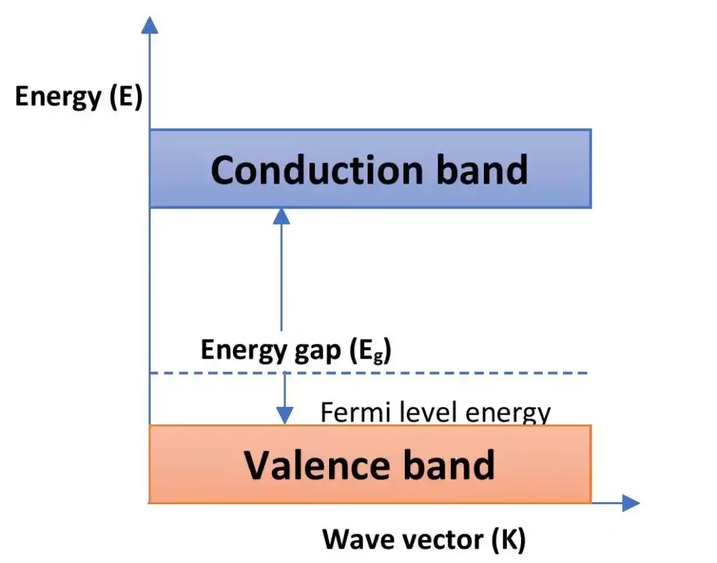
The above figure shows the energy band diagram of p-type semiconductors. For this type of semiconductors, the Fermi level shifts towards the valence band. Because, the density of positive holes becomes higher for p-type semiconductor than its intrinsic counterpart.
Uses of p-type semiconductors
The electrical conductivity of a pure semiconductor is very poor at the room temperature. But we can achieve very high electrical conductivity of the semiconductor due to doping it with impure atoms. Therefore, p-type semiconductors have much higher conductivity even at room temperature. P type of semiconductors can be used to design diodes, transistors, etc. electronic devices.
This is all from this article on p-type of Semiconductors. If you have any doubt on this topic you can ask me in the comment section.
Thank you!
Related posts:

2 thoughts on “p type semiconductor material – formation, properties”
Comments are closed.