Logic gates are the basic components of digital circuits that operates following Boolean algebra. These gates have significant roles in construction of integrated circuits (ICs). There are total seven logic gates in digital electronics. OR gate, AND gate and NOT gate are the three basic logic gates among those. NAND gate and NOR gate are two universal gates. There are two special type logic gates XOR gate and XNOR gate as well. Here, I’m going to discuss the logic circuit and truth table of three basic logic gates only.
What are Logic Gates?
Logic gates are physical electronic devices that can perform logical operations with one or more binary inputs and give a single binary digit at the output. Their function is basically switching operations. All the logic gates are made of resistors and diodes or transistors. Here we are dealing with classical logic gates that obey Boolean algebra. There are some quantum logic gates that are different from these and not the parts of our discussion.
How do the logic gates work?
Logic gates perform classical switching operations. If a logic gate has more than one input, it allows passing the desired binary bit at the output of the logic gate. Even a logic gate can give the complementary of input at the output. Sometimes it gives the complement of the sum or multiplication of the inputs at its output. The constitution elements (Diode or Transistor) of logic gates are designed to be operated as switches, For example, Transistor as a switch.
Logic circuit and Truth table of OR gate
OR gate is a classical logic gate that gives the output as the Boolean sum of the inputs of the gate. An OR gate can have an infinite number of inputs and gives only one output. If A, B, C, D,….. be the inputs of the OR gate then its output will be Y = A+B+C+D+……..
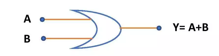
Logic circuit of OR gate using 2 inputs
The following figure is the circuit symbol of OR gate with two inputs A and B.
Truth Table for two Input OR gate
Here is the OR gate truth table with two inputs A and B. The output is taken at Y. Output becomes high if any of the inputs is high. If both inputs are low, then output becomes low.
| Input (A) | Input (B) | Output, Y= A+B |
| 0 | 0 | 0 |
| 0 | 1 | 1 |
| 1 | 0 | 1 |
| 1 | 1 | 1 |
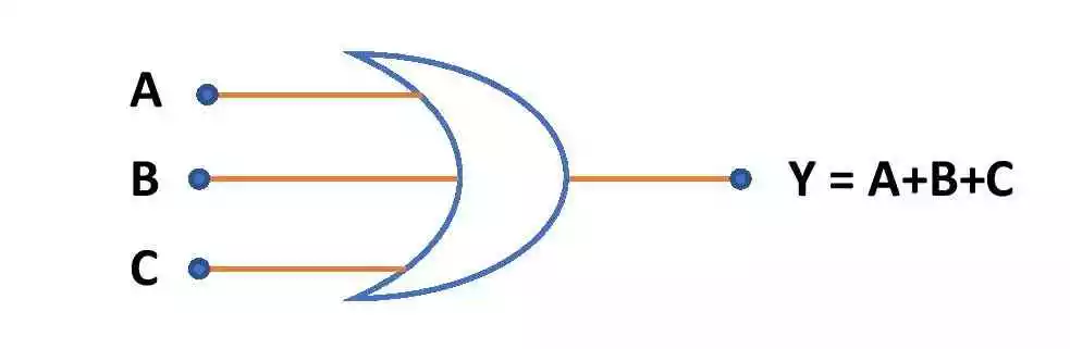
Logic circuit of three input OR gate
This is the circuit symbol of OR gate with three inputs A, B and C.
Truth Table for three Input OR gate
If A, B and C are the inputs then output of OR gate is Y= A+B+C. The truth table is shown below. It suggests that if any of the three inputs is high, the output becomes high.
| Input (A) | Input (B) | Input (C) | Output, Y= A+B+C |
| 0 | 0 | 0 | 0 |
| 0 | 0 | 1 | 1 |
| 0 | 1 | 0 | 1 |
| 0 | 1 | 1 | 1 |
| 1 | 0 | 0 | 1 |
| 1 | 1 | 0 | 1 |
| 1 | 0 | 1 | 1 |
| 1 | 1 | 1 | 1 |
Logic circuit and Truth table of AND gate
AND logic gate is a classical logic gate that gives the output in the form of Boolean multiplication of the inputs. Like OR gate, it can have an infinite number of binary inputs and gives only one output. If A, B, C, D,… be the inputs of AND gate then the Boolean expression for the output will be as Y = A.B.C.D….
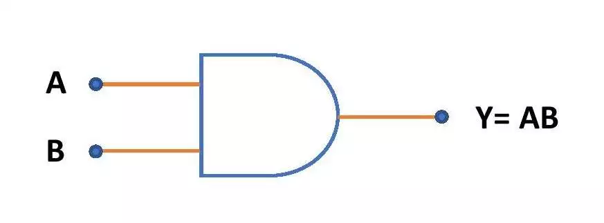
Circuit diagram for two Inputs AND logic gate
The following figure gives the circuit symbol of AND gate with two inputs A and B.
Truth Table for two-input AND gate
Here is the truth table of AND gate with 2 inputs A and B. Output becomes high only when both the inputs are high. Otherwise, it shows low output value.
| Input (A) | Input (B) | Output, Y=AB |
| 0 | 0 | 0 |
| 0 | 1 | 0 |
| 1 | 0 | 0 |
| 1 | 1 | 1 |
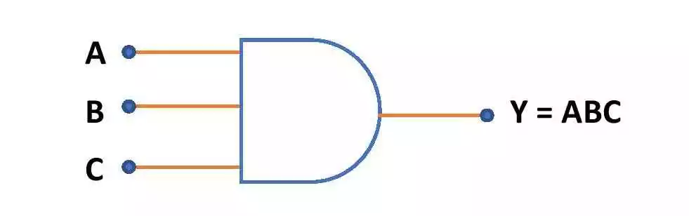
Circuit diagram for three-input AND gate
This is the circuit symbol of AND gate with three inputs A, B and C.
Truth Table for three input AND gate
Here is the truth table of AND gate with 3 inputs A, B and C. When all three inputs are high, the output becomes high.
| Input (A) | Input (B) | Input (C) | Output, Y=ABC |
| 0 | 0 | 0 | 0 |
| 0 | 0 | 1 | 0 |
| 0 | 1 | 0 | 0 |
| 0 | 1 | 1 | 0 |
| 1 | 0 | 0 | 0 |
| 1 | 0 | 1 | 0 |
| 1 | 1 | 0 | 0 |
| 1 | 1 | 1 | 1 |
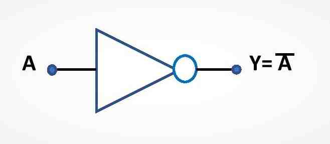
Circuit diagram and Truth table of NOT gate
NOT gate is the classical logic gate that gives the output as the complement of its input. A NOT gate can have only one binary input and it gives the output as the inverter of the input. If we consider that the input of NOT gate is A, then the Boolean expression for the output will be \small \textbf{Y=} \overline{\textbf{A}}. The logic diagram and Truth Table of the NOT gate are given below.
Circuit Symbol for NOT gate
NOT gate has a very simple circuit symbol as shown below. There can be only one input and only one output. The input is A and the output is Y.
Truth Table of NOT gate
| Input (A) | Output \small \textbf{Y=} \overline{\textbf{A}} |
| 0 | 1 |
| 1 | 0 |
Use of Logic gates
- Logic gates have wide applications in logical binary operations.
- Logic gates can store data. Therefore logic circuits like Flipflops, Resisters, counters are used as memory in computers and PCs.
- Switching operation of Logic gates is very much popular. Logic gates are used as switches in digital circuits.
- Logic gates are the main constitutions of integrated circuits (ICs).
These are three fundamental logic gates with truth tables and circuit diagrams. Another way of designing circuit diagrams of basic logic gates is by using NAND gates which are shown in a different article. If you have any doubts in this topic feel free to ask me in the comment section. Thank you!
Related Posts:
- Basic logic gates using NAND gate only
- XOR gate using only NAND gate and only NOR gate
- NAND gate with 3 inputs
- NOR gate
- XNOR gate using NAND and NOR gate only
Comments are closed.